General Description
The RT5717 is a high efficiency synchronous buck converter with typical 60nA ultra-low quiescent current. It provides high efficiency at light loads down to 1µA. Its input voltage range is from 1.8V to 5.5V. The RT5717 provides 16 selectable output voltage levels by connecting a resistor between the RSEL pin and GND while delivering the output current up to 0.75A/1.2A/1.5A. This document explains the function and use of the RT5717P series evaluation board (EVB) and provides information to relate the setting of the evaluation board.
Performance Specification Summary
Table 1 shows the summary of the RT5717P series Evaluation Board performance specification. The ambient temperature is 25°C.
Table 1. RT5717P Series Evaluation Board Performance Specification Summary
|
Specification
|
Test Conditions
|
Min
|
Typ
|
Max
|
Unit
|
|
Input Voltage
|
|
1.8
|
--
|
5.5
|
V
|
|
Output Voltage
|
|
0.5
|
|
4
|
V
|
|
Output Current
|
OCP Select 3
|
--
|
--
|
1.5
|
A
|
|
Operation Frequency
|
|
--
|
1.5
|
--
|
MHz
|
|
Quiescent Current into VIN (Switching)
|
VOUT = 1.8V, EN = VIN = 3.6V,
RSEL = GND
|
--
|
60
|
|
nA
|
|
Shutdown Current
|
EN = GND
|
--
|
20
|
|
nA
|
Power-Up Procedure
Suggestion Required Equipment
- RT5717P series Evaluation Board
- DC power supply capable of at least 5.5V and 3A
- Electronic load capable of 3A
- Function Generator
- Oscilloscope
Quick Start Procedures
The Evaluation Board is fully assembled and tested. Follow the steps below to verify board operation. Do not turn on supplies until all connections are made. When measuring the output voltage ripple, care must be taken to avoid a long ground lead on the oscilloscope probe. Measure the output voltage ripple by touching the probe tip and ground ring directly across the last output capacitor.
Ensure proper measurement equipment setup, then follow the procedure below:
1. Connect JP21 so that the resistor is connected between the RSEL pin and GND to set the output voltage value.
2. With power off, connect the input power supply to the VIN and GND pins.
3. With power off, connect the electronic load between the VOUT and the nearest GND pins.
4. Turn on the power supply at the input. Make sure that the input voltage does not exceed 5.5V on the Evaluation Board.
5. Enabled the RT5717 by the EN pin. When the EN pin is higher than the logic-high threshold, the IC goes to normal operation; When the EN pin transitions from high to low, the device enters shutdown mode. In this state, the converter stops switching, the internal control circuitry is turned off, and the discharge function is triggered.
6. Use a voltmeter to check that the output voltage is correct.
7. Once the correct output voltage is established, adjust the load within the operating ranges and observe the output voltage regulation, ripple voltage, efficiency, and other performance.
Detailed Description of Hardware

Carefully inspect all the components used in the EVB according to the following Bill of Materials table, and then make sure all the components are undamaged and correctly installed. If there is any missing or damaged component, which may occur during transportation, please contact our distributors or e-mail us at evb_service@richtek.com.
Test Points
The EVB is provided with the test points and pin names listed in the table below.
|
Test Point/
Pin Name
|
Function
|
|
VIN
|
Input voltage. (Note VIN on EVB)
|
|
VOUT
|
Output voltage. (Note VOUT on EVB)
|
|
GND
|
Ground. (Note GND on EVB)
|
|
EN
|
Device Enable. (Note EN on EVB)
|
|
SW
|
Switching Signal. (Note SW on EVB)
|
|
RSEL
|
Output Voltage Select. (Note RSEL on EVB)
|
Output Voltage Selection
The RT5717 provides 16 selectable output voltages that can be set with a single external resistor connected between the RSEL pin and GND. The VOUT select circuit starts to detect the value of the resistor when the converter is enabled, and the control circuit is powered up.
Table 2. Output Voltage Setting
|
Type
|
Output-1
|
Output-2
|
Output-3
|
Output-4
|
Output-5
|
RSEL (W)
|
|
Level
|
0.5V to 4V
|
0.8V to 1.55V
|
1.8V to 3.3V
|
1.8V to 3.6V
|
0.54V to 3.7V
|
Min
|
Typ
|
Max
|
|
0
|
0.50
|
0.80
|
1.8
|
1.8
|
--
|
0
|
GND
|
0.01k
|
|
1
|
0.58
|
0.85
|
1.9
|
2.0
|
0.54
|
0.87k
|
0.909k
|
0.95k
|
|
2
|
0.60
|
0.90
|
2.0
|
2.2
|
0.56
|
1.67k
|
1.74k
|
1.81k
|
|
3
|
0.70
|
0.95
|
2.1
|
2.4
|
0.65
|
2.76k
|
2.87k
|
2.98k
|
|
4
|
0.75
|
1.00
|
2.2
|
2.5
|
0.70
|
4.15k
|
4.32k
|
4.49k
|
|
5
|
0.80
|
1.05
|
2.3
|
2.6
|
0.74
|
5.80k
|
6.04k
|
6.28k
|
|
6
|
1.10
|
1.10
|
2.4
|
2.7
|
1.00
|
8.11k
|
8.45k
|
8.79k
|
|
7
|
1.20
|
1.15
|
2.5
|
2.8
|
1.10
|
11.04k
|
11.5k
|
11.96k
|
|
8
|
1.50
|
1.20
|
2.6
|
2.9
|
1.40
|
15.17k
|
15.8k
|
16.43k
|
|
9
|
1.60
|
1.25
|
2.7
|
3.0
|
1.50
|
20.64k
|
21.5k
|
22.36k
|
|
10
|
1.80
|
1.30
|
2.8
|
3.1
|
1.65
|
27.55k
|
28.7k
|
29.85k
|
|
11
|
1.90
|
1.35
|
2.9
|
3.2
|
1.75
|
36.77k
|
38.3k
|
39.83k
|
|
12
|
2.10
|
1.40
|
3.0
|
3.3
|
1.95
|
50.21k
|
52.3k
|
54.39k
|
|
13
|
3.00
|
1.45
|
3.1
|
3.4
|
2.80
|
68.64k
|
71.5k
|
74.36k
|
|
14
|
3.30
|
1.50
|
3.2
|
3.5
|
3.05
|
97.92k
|
102k
|
106.08k
|
|
15
|
4.00
|
1.55
|
3.3
|
3.6
|
3.70
|
256.32k
|
267k
|
277.68k
|
Note 1: E96 resistor series, 1% accuracy, temperature coefficient better or equal than ±200 ppm/°C.
Bill of Materials
|
Reference
|
Count
|
Part Number
|
Value
|
Description
|
Package
|
Manufacturer
|
|
U1
|
1
|
RT5717P series
|
RT5717P
|
Buck Converter
|
XWL-CSP-6B 0.96X1.245(mm2)
|
RICHTEK
|
|
C1
|
1
|
GRM21BR61A476ME15L
|
47µF
|
47µF/6.3V/X5R
|
0805(inch)
|
Murata
|
|
C3
|
1
|
GRM155R60J475ME47D
|
4.7µF
|
4.7µF/6.3V/X5R
|
0402(inch)
|
Murata
|
|
C4
|
1
|
GRM155R60J106ME15
|
10µF
|
10µF/6.3V/X5R
|
0402(inch)
|
Murata
|
|
L1
|
1
|
DFE201610E-1R0M
|
1uH
|
1uH
|
0805(inch)
|
Murata
|
|
R3
|
1
|
Resistor E96 series
|
See Table 2
|
1%, TC ±200ppm
|
0201(inch)
|
|
Typical Applications
EVB Schematic Diagram
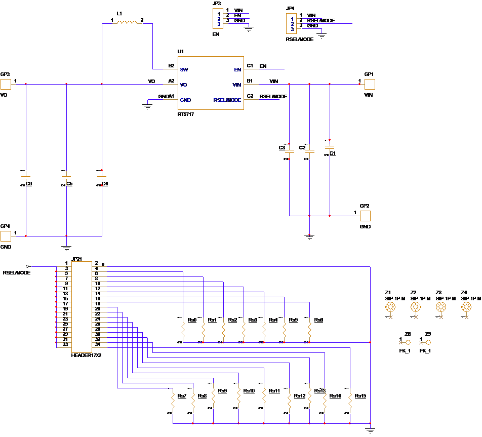
1. The capacitance values of the input and output capacitors will influence the input and output voltage ripple.
2. MLCC capacitors have degrading capacitance at DC bias voltage, and especially smaller size MLCC capacitors will have much lower capacitance.
Measure Result
|
No Load Operating Quiescent Current
vs. Input Voltage
|
Shutdown Current vs. Input Voltage
|
|

|

|
|
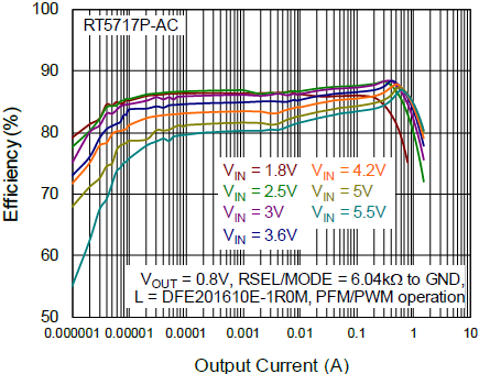
Efficiency, Power Save Mode
|
Efficiency, Power Save Mode
|
|
|

|
|
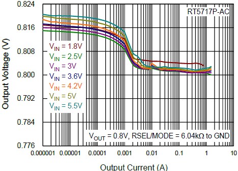
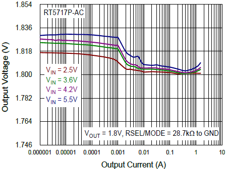
Output Voltage vs. Output Current
|
Output Voltage vs. Output Current
|
|
|
|
|
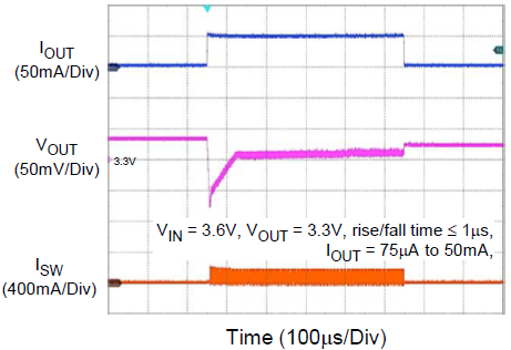
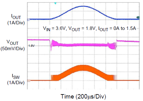
Load Transient PSM Mode
|
Load Transient PSM Mode
|
|

|
|
|
Load Transient PSM Mode
|
AC Load Sweep Power Save Mode
|
|

|
|
|
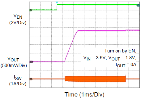
Start-Up
|
Output Discharge
|
|
|

|
Note 2. When measuring the input or output voltage ripples, care must be taken to avoid a long ground lead on the oscilloscope probe. Measure the output voltage ripple by touching the probe tip directly across the output capacitor.
Evaluation Board Layout
Figure 1 to Figure 4 show the layout of the RT5717P series Evaluation Board. This board size is 56mm x 50mm and is constructed on four-layer PCB, outer layers with 1 oz. Cu, and inner layers with 1 oz. Cu.
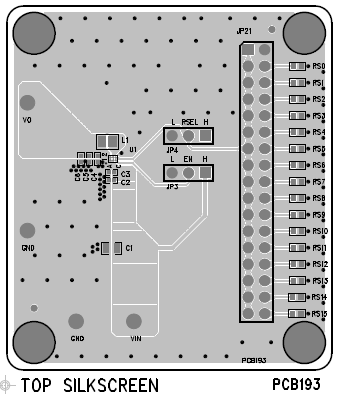
Figure 1. Top View (1st layer)
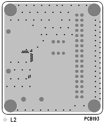
Figure 2. PCB Layout—Inner Side (2nd Layer)
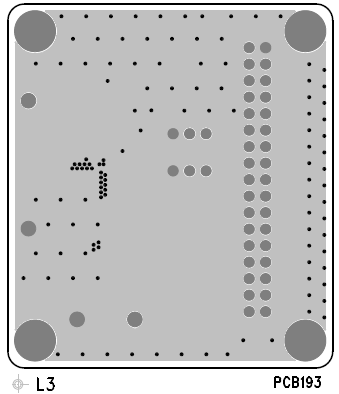
Figure 3. PCB Layout—Inner Side (3rd Layer)
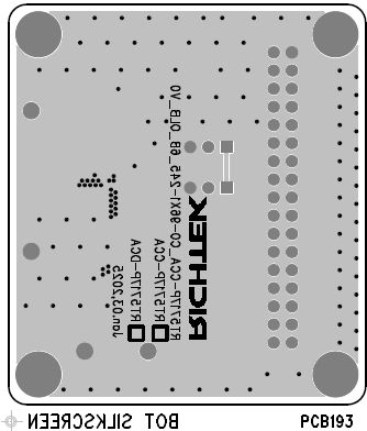
Figure 4. Bottom View (4th Layer)
More Information
For more information, please find the related datasheet or application notes from Richtek website http://www.richtek.com.
Important Notice for Richtek Evaluation Board
THIS DOCUMENT IS FOR REFERENCE ONLY, NOTHING CONTAINED IN THIS DOCUMENT SHALL BE CONSTRUED AS RICHTEK’S WARRANTY, EXPRESS OR IMPLIED, UNDER CONTRACT, TORT OR STATUTORY, WITH RESPECT TO THE PRESENTATION HEREIN. IN NO EVENT SHALL RICHTEK BE LIABLE TO BUYER OR USER FOR ANY AND ALL DAMAGES INCLUDING WITHOUT LIMITATION TO DIRECT, INDIRECT, SPECIAL, PUNITIVE OR CONSEQUENTIAL DAMAGES.